|
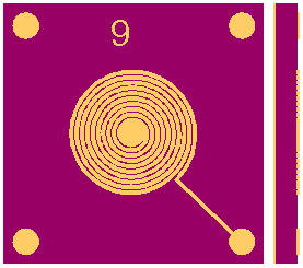
SPIRAL CHIP INDUCTORS LX3000Q20-L09-50nH FEATURES Spiral chip inductors are available in 2 different die dimensions: For
1 turn to 21 turns series the die size is 0.030"x0.030"x0.020". For 1 turn to 5.5 turns the spiral chip inductors are also
available in die size of 0.030"x0.030"x0.020". The L09-50nH spiral chip inductors are manufactured on quartz (SiO2), 20
mils thick. APPLICATIONS These devices can be used over the full military temperature range -55°C to +125°C. Quality and workmanship
is per MIL-S-883. Devices are 100% tested, visual inspected and packaged in waffle packs. Spiral Chip Inductors Lab kits are
available from stock: L-Kit Application note: AN 102 PRODUCT DESCRIPTION The L09-50nH Series of spiral chip inductors
are designed to be used in chip and wire hybrid circuits as RF choke in power supplies and microwave circuit resonant elements.
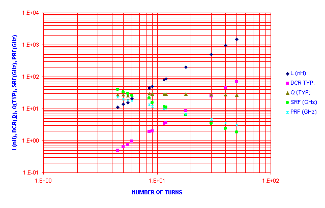
When used as chokes, a modest Q is desirable while in oscillators Q has to be as high as possible. Semiconwell advanced
thin film technologies allow for an important reduction of the DCR max, which translates into an increased Q. For spirals
with w+s=25µm, Q values between 25 and 30 are obtained which represent a better compromise between the two applications. For
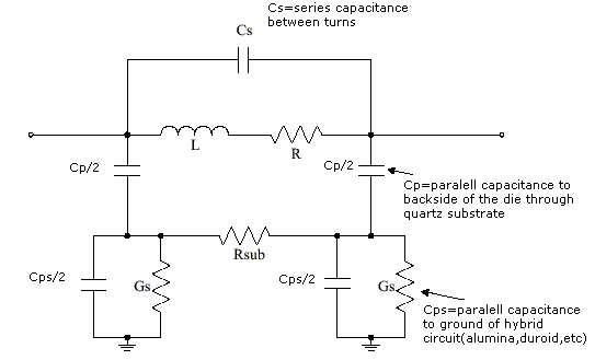
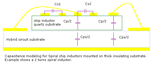
lowest capacitance and higher self resonance, the L09-50nH spiral chip inductors are manufactured on 20 mil thick quartz
(SiO2) substrates. Application note AN 102 describes the recommended assembly for best performance. MICROWAVE APPLIED THIN
FILM PRODUCTS MANUFACTURING PROCESS DESCRIPTION All thin film microwave products are manufactured using advanced thin film
technologies including ultra-stable and self passivating Tantalum Nitride resistors, gold interconnect metallization and reliable
MNOS capacitors to achieve excellent uniformity, performance and reliability. Thin film technology is the preferred solution
for all applications that require low noise, long term stability and excellent performance at very high frequencies. Semiconwell
employs proprietary thin film technologies for deposition of a wide range of sheet resistance films from 1W/sq to 10,000 W/sq.
All Semiconwell products are available in die form and are ideal for high reliability hybrid and multi chip module applications.
SUBSTRATE INFORMATION INDUCTOR SPECIFICATIONS Material SiO2 -Quartz Thickness 20±1 mil Die size 30x30&plswn;3 mils, 30x30&plswn;3
mils Current rating 100mA@70°CTolerance 20 % Capacitance <0.030pF CONDUCTORS The conductor and bonding pads are 3µm
thick, 99.99% electroplated gold with a TiW barrier that withstands 30 min at 400°C in air without loss of adhesion. BACKSIDE
METALS Backside of the die is NOT metallized. Standard TiW/Au or custom metallization is available for special orders. ELECTRICAL
CHARACTERISTICS Inductance 50nH , Inductance Tolerance (Absolute) + 25°C ±20.0 % DC Resistance typ. 0.1W
Current Rating: Max. 100mA@70°C Quality Factor Q @ 100MHz typ. 25.5 Series Self Resonance SRF typ. ff GHz Parallell Self
Resonance PRF typ. ff GHz Operating Temperature Range - 55 to + 125°C Storage Temperature Range - 55 to + 125°C PRICES,
DELIVERY & ORDERING INFORMATION PART# L01-01nH Minim Order 100pc U/P($) $3.20 All Semiconwell products are available
in die form. Typical delivery for die products is 1-2 weeks ARO. For Custom designs, delivery is 2-3 weeks ARO. Certain items
may be available from stock. Inventory is periodically updated. All devices for chip and wire applications are shipped in
waffle packs. Semiconwell has made every effort to have this information as accurate as possible. However, no responsibility
is assumed by Semiconwell for its use, nor for any infringements of rights of third parties which may result from its
use. Semiconwell reserves the right to revise the content or modify its product line without prior notice. Semiconwell
products are not authorized for and should not be used within support systems which are intended for surgical implants into
the body, to support or sustain life, in aircraft, space equipment, submarine, or nuclear facility applications without the
specific written consent of Semiconwell. |