|
Vishay PRN1645 same as SWRN1645 THIN FILM DIFFERENTIAL TERMINATION
RESISTOR NETWORKS pin to pin compatible with PRN1645 manufactured
by SEMICONWELL. PRN 1645, SCSI Termination resistor networks, SCSI
Termination, SCSI Terminator, Custom,Resistor Networks, Resistor-Capacitor
Networks,Schottky diodes,EMI Filters,Clamp Termination Networks,ESD
Protection Circuits,isolated,bussed,terminations, EMI,RFI,ESD,TVS,clamp,protection,
RC networks, power resistors,level shifter, low pass filters, schottky diodes,
resistor networks, voltage divider,voltage reference, SCSI terminator,
matching network SEMICONWELL Integrated Passive Networks THIN FILM DIFFERENTIAL TERMINATION RESISTOR NETWORKS
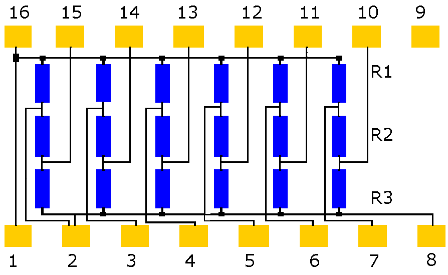
SWRN1645 FEATURES APPLICATIONS SCHEMATIC
0.190" [4.83mm] maximum seated height
Rugged, molded case construction
Low temperature coefficient ±100 ppm/°C
Compatible with automatic insertion equipment
Thin film resistive elements
Reduces PC board space and reduces total assembly costs
TTL to ECL translatorr
SHORT PRODUCT APPLICATION NOTE
The SWRN1645 is a high performance Integrated Device designed to eliminate
trensmission line effects on high-speed lines on a TTL. TTL is a bus interface
covered by ANSI standard that allows for an input/output bus to connect small
computers with a variety of peripheral devices. Proper resistor termination
requires a resistor whose value closely matches the characteristic impedance
of the transmisision line. Thin film networks offer significant advantage over
thick film processes in terms of tighter absolute and ratio tolerances, lower noise,
lower Temperature Coefficient of Resistance, greater stability. They offer
superior high frequency performance with minimal parasitic inductance and
capacitance. Integrated thin film networks also offer the benefits of board space
savings, reduced assembly costs, and increased reliability with fewer components.
SEMICONDUCTOR-THIN FILM MANUFACTURING PROCESS DESCRIPTION
Integrated passive networks are manufactured using advanced thin film technologies
including ultra -stable and self passivating Tantalum Nitride resistors, gold interconnect
metallization and reliable MNOS capacitors to achieve excellent uniformity, performance
and reliability. Thin film resistor technology is the preferred solution for all applications that
require low noise, long term stability and excellent performance at very high frequencies.
Semiconwell employs proprietary thin film technologies for deposition of a wide range of
sheet resistance films from 1 W/sq to 10,000 W/sq. All Semiconwell's products are available
in die form and as KGD, known good die and are ideal for high reliability hybrid and multi
chip module applications. Besides thin film resistors, Semiconwell integrates capacitors,
Schottky diodes, Zener diodes and transistors. Integrated passive and active networks
are manufactured using Semiconwell's in house high reliability semiconductor manufacturing processes.
All semiconductor devices employ precision doping via ion implantation, silicon nitride junction passivation,
platinum silicided contacts and gold interconnect metallization for best performance and reliability.
MNOS capacitors and Tantalum Nitride resistors are easily integrated with Schottky diode
to provide complete standard and custom RCD solutions. In die form, these products
are ideal for hybrid and multi chip module applications. In packaged form, these
products are the best solution where space and weight are a concern.
RESISTOR SPECIFICATIONS Capacitance [pF] Tolerance q [%] Power Rating [mW]
< 5pF 5 125mW@70°C
Stresses beyond listed absolute maximum ratings may cause permanent damage to the device.
PARAMETER VALUE UNITS
Resistors standard value R1 R2 R3 180 270 820 W WW
Operating Temperature Range
-55 to 125°C
Temperature Coefficient of Resistance
±100 ppm/°C
Noise, (MIL-STD-202, Method 308)
max. -25dB GENERAL DIE INFORMATION
Substrate Thickness (mils) Die size (mils) Bonding pads Backside metal
SiO2 / Silicon 10±2 90 x 60 ±3 4x4 mils, 3mm thick, 99.99%
electroplated gold with a TiW barrier Au/Si compatible with eutectic and conductive epoxy die attach.
All Semiconwell products are available in die form for chip and wire hybrid
circuits and multi chip modules applications. Typical delivery for standard
die products is 3-4 weeks ARO. For Chip Scale Packaged (CSP) devices consult
factory for an update on availability of certain products.
CONDUCTORS RESISTORS BACKSIDE METAL
The bonding pads of the resistors are 3µm thick, 99.99% electroplated gold
with a TiW barrier that withstands 30 min at 400°C in air without loss of adhesion.
Resistive material is ultra stable TaN with low TCR < 75ppm/°C typical. For Rsq< 10W/sq and Rsq>
500W/sq, the resistive material is proprietary. Power rating/resistor max 100mW for R< 1KW and 25mW for R>1KW.
Standard tolerance is ±5%. Backside of the die is metallized with standard Si/Au
compatible with eutectic and epoxy die attach. Custom metallizations are available
upon special request for die products only.
DIE LAYOUT PACKAGE PIN OUT
Vin=10,11,12,13,14,15
Vss=2,3,4,5,6,7
VCC=1,16
GND=8 STANDARD PRODUCTS ORDERING INFORMATION
R1(W) R2(W) R3(W) R CODE SOT23 BARE DIE
180 270 820 180/270/820 SWRN1645/R180/R270/R820-16SO SWRN1645/R180/R270/R820-BD
10 to 10M 10 to 10M 10 to 10M /XXX/XXX/XXX SWRN/XXX/XXX-ST SWRN-XXX/XXX-BD
SW PART # QUANTITY U/P($) BARE DIE U/P($)
SWRN1645/RCODE-10% 5,000pc - -BD
SWRN1645/RCODE-10% 10,000pc - -BD
SWRN1645/RCODE-5% 5,000pc - -BD
SWRN1645/RCODE-5% 10,000pc - -BD
SWRN1645/RCODE-1% 5,000pc - -BD
SWRN1645/RCODE-1% 10,000pc - -BD
For custom products sold as bare tested die or known good die KGD, minimum
order is 5000pc. Dice are 100% functional tested, visual inspected and shipped in
antistatic waffle packs. For special die level KGD requirements, different packaging
or custom configurations, contact sw_sales@semiconwell.com
CUSTOM PRODUCTS ORDERING INFORMATION - P/N BUILDER
R1 R1 multiplier R2 R2 multiplier R3 R3 multiplier Tolerance Package
Find part # INSTANT QUOTE
Semiconwell P/N Quantity E-mail
Delivery for packaged Resistor networks standard products is 4-6
weeks ARO. Certain items may be available from stock. For standard
products available from stock, there is a minimum line item order of
$250.0. Inventory is periodically updated. For 2500pc or larger orders,
all surface mount packaged devices are shipped in tape on reel (T/R).
For smaller quantities, it may vary. Samples are available only for customers
that have issued firm orders pending qualification of product in a particular
application. On line Orders have to be verified, accepted and acknowledged
by Semiconwell sales department in writing before, becoming non cancelable binding contracts.
Semiconwell guarantees continuous supply and availability of any of it's standard products provided minimum order quantities are met.
SEMICONWELL has made every effort to have this information as accurate
as possible. However, no responsibility is assumed by SEMICONWELL for its use,
nor for any infringements of rights of third parties which may result from its use.
SEMICONWELL reserves the right to revise the content or modify its product line
without prior notice. SEMICONWELL products are not authorized for and should
not be used within support systems which are intended for surgical implants into
the body, to support or sustain life, in aircraft, space equipment, submarine, or
nuclear facility applications without the specific written consent.
Home Product Tree Tech. Support Print PDF Packages Request Quote Inventory Place Order Contact sales
Home>Resistor Arrays>SWRN1645> Last updated: December 11, 2006
SEMICONWELL www.semiconwell.com Tel:(408)986-8026 Fax:(408)986-8027
©1990-2006 SEMICONWELL All rights reserved. No material from this site may be used or reproduced without permission. |