| FEATURES |
| APPLICATIONS |
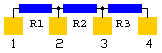
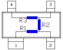
| SCHEMATIC |
| Wide resistance range 10 to 1MΩ |
| Tolerance ±0.1%, ratios ±0.05% |
| Low temperature coefficient ±25ppm/°C |
| Long term stability, 0.05% after 1000 hours |
| Also available in custom values and configuration |
| Precision voltage divider |
| OP AMP gain control |
| Precise Attenuation |
| Pull-up/pull-down |
| TTL/MOS interfacing |
| Linear Technology Pentium 54/55 Power Supply Regulator |