|
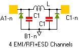
4 CHANNELS LCD AND CAMERA EMI FILTER ARRAY WITH ESD PROTECTION SWCM1452-04-CSP
FEATURES APPLICATIONS SCHEMATIC
4 channels of EMI filtering LCD and Camera data lines in mobile handsets
Greater than 30dB of attenuation at 1GHz EMI filtering for data ports in cell phones, PDAs or notebook computers
15kV ESD protection(IEC 61000-4-2, contact discharge) I/O port protection for mobile handsets, notebook computers, PDAs etc.
30kV ESD protection (HBM) EMI filtering for LCD and chip-to-chip data lines in mobile electronic devices that use flexible PCB interconnections
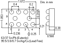
Chip Scale Package (CSP) with 0.40mm pitch and 0.25mm CSP solder ball which features extremely low parasitic inductance for optimum filter and ESD performance
SHORT PRODUCT APPLICATION NOTE
SWCM1452 is a family of pi-style EMI filter arrays with ESD protection, which integrates four, six and eight filters (C-L-C) in CSP form factor with 0.40mm pitch. Each EMI filter channel of the CM1452 is implemented as a 3-pole L-C filter where the component values are 20pF-17nH-20pF. The SWCM1452’s roll-off frequency at -6dB attenuation is 330MHz and can be used in applications where the data rates are as high as 132Mbps while providing greater than 30dB over the 800MHz to 2.7GHz frequency range. The parts include ESD diodes on every I/O pin, which provide a very high level of protection for sensitive electronic components that may be subjected to electrostatic discharge (ESD). The ESD protection diodes connected to the filter ports are designed and characterized to safely dissipate ESD strikes of 15kV, beyond the maximum requirement of the IEC61000-4-2 international standard. Using the MIL-STD-883 (Method 3015) specification for Human Body Model (HBM) ESD, the pins are protected for contact discharges at greater than 30kV. This device is particularly well suited for wireless handsets, mobile LCD modules and PDAs because of its small package format and easy-to-use pin assignments. In particular, the SWCM1452 is ideal for EMI filtering and protecting data and control lines for the LCD display and camera interface in mobile handsets.The SWCM1452 is available in a space saving, low profile Chip Scale Package with optional lead-free finishing (95.5Sn/3.8Ag/0.7Cu). It is manufactured with a 0.40mm pitch and 0.25mm CSP solder ball to provide up to 28% board space savings vs. competing CSP devices with 0.50mm pitch and 0.30mm CSP solder ball..
SEMICONDUCTOR-THIN FILM MANUFACTURING PROCESS DESCRIPTION
Integrated passive networks are manufactured using advanced thin film technologies including ultra -stable and self passivating Tantalum Nitride resistors, gold interconnect metallization and reliable MNOS capacitors to achieve excellent uniformity, performance and reliability. Thin film resistor technology is the preferred solution for all applications that require low noise, long term stability and excellent performance at very high frequencies. Semiconwell employs proprietary thin film technologies for deposition of a wide range of sheet resistance films from 1W/sq to 10,000 W/sq. All Semiconwell's products are available in die form and as KGD, known good die and are ideal for high reliability hybrid and multi chip module applications. Besides thin film resistors, Semiconwell integrates capacitors, Schottky diodes, Zener diodes and transistors. Integrated passive and active networks are manufactured using Semiconwell's in house high reliability semiconductor manufacturing processes. All semiconductor devices employ precision doping via ion implantation, silicon nitride junction passivation, platinum silicided contacts and gold interconnect metallization for best performance and reliability. MNOS capacitors and Tantalum Nitride resistors are easily integrated with Schottky diodes to provide complete standard and custom RCD solutions. In die form, these products are ideal for hybrid and multi chip module applications. In packaged form, these products are the best solution where space and weight are a concern.
ABSOLUTE MAXIMUM RATINGS
Operating Temperature Range,°C Storage Temperature Range,°C Current per Inductor DC Package Inductor
-40to+85 -65 to +150 30mA 0.5W
Stresses beyond listed absolute maximum ratings may cause permanent damage to the device.
ELECTRICAL CHARACTERISTICS
PARAMETER VALUE UNITS
Channel Inductance typ.17 nH
Total Channel Capacitance at 2.5Vdc; 1MHz, 30mVac min.32 typ.40 max.48 pF
Capacitance C1 at 2.5V dc; 1MHz, 30mV ac min.16 typ.20 max.24 pF
Cut-off Frequency, ZSOURCE = 50 , ZLOAD = 50 typ.148 MHz
Roll-off Frequency at -6dB Attenuation, ZSOURCE = 50,ZLOAD = 50 typ.330 MHz
Stand-off Voltage, I = 10mA min. 5.5 V
Diode Leakage at 3.3V reverse bias voltage typ.0.1 max. 1.0 µA
Signal Clamp Voltage: Positive Clamp, 10mA Negative Clamp, -10mA min.5.6 typ.6.8 max.9.0 min.-1.5 typ.-0.8 max.-0.4 V V
In-system ESD withstand voltage(Note 1): Human Body Model (MIL-STD-883, method 3015) IEC 61000-4-2, contact discharge method min.30 min.15 kV kV
Dynamic Resistance Positive Negative typ. 2.3 typ. 0.9 W W
Note 1: ESD applied to input/output pins with respect to GND, one at a time. Clamping voltage is measured at the opposite side of the EMI filter to the ESD pin (i.e. if ESD is applied to pin A1 then clamping voltage is measured at pin C1). Unused pins are left open. These parameters are guaranteed by design.
GENERAL DIE INFORMATION
Substrate Thickness (mils) Die size (mils) Bonding pads Backside metal
SiO2 / Silicon 15±2 65.8x41.5±3 0.25mm CSP solder balls with 0.40mm pitch 63/37 Sn/Pb (Eutectic)or 95.5/3.8/0.7 Sn/Ag/Cu (Lead-free)
All Semiconwell products are available in die form for chip and wire hybrid circuits and multi chip modules applications. Typical delivery for standard die products is 3-4 weeks ARO. For Chip Scale Packaged (CSP) devices consult factory for an update on availability of certain products.
DIODES RESISTORS CAPACITORS
The diodes offer basic ESD protection, with low forward voltage, low leakage and low power dissipation in OFF state.Diodes exhibit low junction capacitance CTand low on resistance RDON. Ultra stable TaN with low TCR <75ppm/°C typical. For Rsq<10W/sq and Rsq>500W/sq, resistive material is proprietary. Power rating/resistor max 100mW for R<1KW and 25mW for R>1KW. Standard tolerance is ±5%. Silicon nitride dielectric, MNOS capacitors exhibit high stability, low temperature coefficients, low leakage <10nA and high BV>50V.
DIE LAYOUT PACKAGE PIN OUT
A1-Filter1,A2-Filter2,A3-Filter3,A4-Filter4
C1-Filter1,C2-Filter2,C3-Filter3,C4-Filter4
B1,B2-GND
STANDARD PRODUCTS ORDERING INFORMATION
SW PART # QUANTITY CSP-10 U/P($) BARE DIE U/P($)
SWCM1452-04 5,000pc -10CSP -10BD
SWCM1452-04 10,000pc -10CSP -10BD
For products sold as bare tested die or known good die KGD, minimum order is 5000pc. Dice are 100% functional tested, visual inspected and shipped in antistatic waffle packs. For special die level KGD requirements, different packaging or custom configurations, contact sw_sales@semiconwell.com
Top of Form 1
Semiconwell P/N Quantity E-mail
Receive Instant Quote
Bottom of Form 1
Delivery for packaged RCD standard products is 6-8 weeks ARO. Certain items may be available from stock. For standard products available from stock, there is a minimum line item order of $250.0. Inventory is periodically updated. For 2500pc or larger orders, all surface mount packaged devices are shipped in tape on reel (T/R). For smaller quantities, it may vary. Samples are available only for customers that have issued firm orders pending qualification of product in a particular application. On line Orders have to be verified, accepted and acknowledged by Semiconwell sales department in writing before, becoming non cancelable binding contracts.
Semiconwell guarantees continuous supply and availability of any of it's standard products provided minimum order quantities are met.
SEMICONWELL has made every effort to have this information as accurate as possible. However, no responsibility is assumed by SEMICONWELL for its use, nor for any infringements of rights of third parties which may result from its use. SEMICONWELL reserves the right to revise the content or modify its product line without prior notice. SEMICONWELL products are not authorized for and should not be used within support systems which are intended for surgical implants into the body, to support or sustain life, in aircraft, space equipment, submarine, or nuclear facility applications without the specific written consent.
|