Data I/O Port EMI/RFI PI Filter ESD Protected SWPIESDE1channel of EMI filtering for data ports Pi-style EMI filters in a capacitor-resistor-capacitor (C-R-C) network Greater than 32dB attenuation at 1 GHz ±15kV ESD protection on each channel (IEC 61000-4-2 Level 4, contact discharge) ±30kV ESD protection on each channel (HMB) EMI filtering and ESD protection for both data and I/O ports 
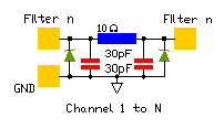
Wireless Handsets Handheld PCs/PDAs MP3 Players Notebooks Desktop PCs The SWPIESDE is a one to eight channels low-pass filter array that reduces EMI/RFI emissions while at the same time providing ESD protection. It is used on data ports on mobile devices. To reduce EMI/RFI emissions, the SWESDE integrates a pi-style filter (C-R-C) for each channels.Each high quality filter provides greater than 30dB attenuation in the 800-2700 MHz range. These pi-style filters also support bidirectional filtering, controlling EMI both to and from a data port connector. In addition , the SWPIESDE provides a very high level of protection for sensitive electronic components that may be subjected to electrostatic discharge (ESD). The input pins are designed and characterized to safely dissipate ESD strike of 15kV, exceeding the maximum requirement of the IEC 61000-4-2 international standard. Using the MIL-STD-883 (Method 3015) specification for Human Body Model (HBM) ESD, the device provides protection for contact discharges to greater than 30kV. The SWPIESDE is particularly well suited for portable electronics (e.g., cellular telephones, PDAs, notebook computers) because of its small package format and low weight. Integrated passive networks are manufactured using advanced thin film technologies including ultra-stable and self passivating Tantalum Nitride resistors, gold interconnect metallization and reliable MNOS capacitors to achieve excellent uniformity, performance and reliability. Thin film resistor technology is the preferred solution for all applications that require low noise, long term stability and excellent performance at very high frequencies. Semiconwell employs proprietary thin film technologies for deposition of a wide range of sheet resistance films from 1W/sq to 10,000 W/sq. All Semiconwell's products are available in die form and are ideal for high reliability hybrid and multi chip module applications. Semiconwell manufactures passive network components, integrated active and passive devices, resistor networks, capacitor networks, schottky and zener diode networks, and npn, pnp transistors arrays that perform the following functions: series and parallel linear and nonlinear GTL, AC, Diode, Thevenin termination networks, precision thin film resistor capacitor networks (RC networks), isolated, bussed resistor networks including zero ohms jumper arrays, voltage divider networks, resistor networks for audio applications, EMI, RFI and ESD zener clamped diodes and transient voltage suppressors networks, EMI/RFI filter networks and clock terminations. Semiconwell's proprietary semiconductor technology, advanced thin films processes, in house assembly and packaging technologies allow manufacturing of flip chip CSP chip scale and MLF molded lead frame surface mount integrated passive networks that include unprecedented large capacitors >1microfarad (1µF) and giga ohms resistors (GW).


SEMICONWELL
Integrated Passive Networks
  DATA I/O PORT EMI/RFI PI FILTER ESD PROTECTED
SWPIESDE-N


FEATURES
APPLICATIONS
SCHEMATIC
1to 14 channels of EMI filtering for data ports
Pi-style EMI filters in a capacitor-resistor-capacitor (C-R-C) network
Greater than 32dB attenuation at 1 GHz
±15kV ESD protection on each channel (IEC 61000-4-2 Level 4, contact discharge)
±30kV ESD protection on each channel (HMB)
 
EMI filtering and ESD protection for both data and I/O ports
Wireless Handsets
Handheld PCs/PDAs
MP3 Players
Notebooks
Desktop PCs
schematic

SHORT PRODUCT APPLICATION NOTE
The SWPIESDE is a one to eight channels low-pass filter array that reduces EMI/RFI emissions while at the same time providing ESD protection. It is used on data ports on mobile devices. To reduce EMI/RFI emissions, the SWESDE integrates a pi-style filter (C-R-C) for each channels.Each high quality filter provides greater than 30dB attenuation in the 800-2700 MHz range. These pi-style filters also support bidirectional filtering, controlling EMI both to and from a data port connector. In addition , the SWPIESDE provides a very high level of protection for sensitive electronic components that may be subjected to electrostatic discharge (ESD). The input pins are designed and characterized to safely dissipate ESD strike of 15kV, exceeding the maximum requirement of the IEC 61000-4-2 international standard. Using the MIL-STD-883 (Method 3015) specification for Human Body Model (HBM) ESD, the device provides protection for contact discharges to greater than 30kV. The SWPIESDE is particularly well suited for portable electronics (e.g., cellular telephones, PDAs, notebook computers) because of its small package format and low weight.

SEMICONDUCTOR-THIN FILM MANUFACTURING PROCESS DESCRIPTION
Integrated passive networks are manufactured using advanced thin film technologies including ultra -stable and self passivating Tantalum Nitride resistors, gold interconnect metallization and reliable MNOS capacitors to achieve excellent uniformity, performance and reliability. Thin film resistor technology is the preferred solution for all applications that require low noise, long term stability and excellent performance at very high frequencies. Semiconwell employs proprietary thin film technologies for deposition of a wide range of sheet resistance films from 1W/sq to 10,000 W/sq. All Semiconwell's products are available in die form and as KGD, known good die and are ideal for high reliability hybrid and multi chip module applications. Besides thin film resistors, Semiconwell integrates capacitors, Schottky diodes, Zener diodes and transistors. Integrated passive and active networks are manufactured using Semiconwell's in house high reliability semiconductor manufacturing processes. All semiconductor devices employ precision doping via ion implantation, silicon nitride junction passivation, platinum silicided contacts and gold interconnect metallization for best performance and reliability. MNOS capacitors and Tantalum Nitride resistors are easily integrated with Schottky diodes to provide complete standard and custom RCD solutions. In die form, these products are ideal for hybrid and multi chip module applications. In packaged form, these products are the best solution where space and weight are a concern.

ABSOLUTE MAXIMUM RATINGS
Reverse voltage VR Continuous IF IFRM for tw<100ms Max Power dissipation
7V 100mA 200 mA (20%duty cycle) 100mW@70°C/channel

Stresses beyond listed absolute maximum ratings may cause permanent damage to the device.

ELECTRICAL CHARACTERISTICS
PARAMETER VALUE UNITS
Storage Temperature Range
-65 to +150
°C
Operating Temperature Range
-40 to +85
°C
DC Power per Resistor
100
mW
DC Package Power Rating
600
mW
Resistance
min. 80 typ.100 max.120
W
Capacitance , at 2.5VDC
min.24 typ.30 max.36
pF
Temperature Coefficient of Resistance
typ.1200
ppm/°C
Temperature Coefficient of Capacitance , at 2.5 VDC
-300
ppm/°C
Diode Voltage,reverse bias, Idiode=10 mA
min.5.5
V

Signal Voltage, Positive Clamp,I LOAD = 10mA
Signal Voltage,Negative Clamp

min.5.6 ; typ.6.8; max.9
min.-0.4;typ.-0.8;max.-1.5

V
V

In-system ESD Withstand Voltage,Notes 2,4 and 5
a) Human Body Model, MIL-STD-883,Method 3015
b) Contact Discharge per IEC 61000-4-2 Level 4

min. ±30
min. ±15

kV
kV

Clamping Voltage during ESD Discharge MIL-STD-883 (Method 3015), 8kV;Notes 2,3,4 and 5
Positive Transients
Negative Transients


typ. +10
typ. -5


V
V

Note 1: T A =25°C unless otherwise specified
Note 2: ESD applied to input and output pins with respect to GND, one at a time.
Note 3: Clamping voltage is measured at the opposite side of the EMI filter to the ESD pin.
Note 4: Unused pins are left open
Note 5: The parameters are guaranteed by design and characterization.


GENERAL DIE INFORMATION
Substrate Thickness (mils) Die size (mils) Bonding pads Backside metal
Silicon 10±2 43 x 82 ±3 4x4 mils, 3µm thick, 99.99% electroplated gold with a TiW barrier Au/Si compatible with eutectic and conductive epoxy die attach.
All Semiconwell products are available in die form for chip and wire hybrid circuits and multi chip modules applications. Typical delivery for standard die products is 3-4 weeks ARO. For Chip Scale Packaged (CSP) devices consult factory for an update on availability of certain products.

DIODES RESISTORS CAPACITORS
The protection diodes use solid state silicon avalanche technology and are characterized by their high surge capability, low operating and clamping voltages, fast response time and low leakage current Ultra stable TaN with low TCR <75ppm/°C typical. For Rsq<10W/sq and Rsq>500W/sq, resistive material is proprietary. Power rating/resistor max 100mW for R<1KW and 25mW for R>1KW. Standard tolerance is ±5%. Silicon nitride dielectric, MNOS capacitors exhibit high stability, low temperature coefficients, low leakage <10nA and high BV>50V.

DIE LAYOUT PACKAGE PIN OUT
schematic
Vin=3,4,5,6,11,12,13,14
Vss=die backside
Vss=1,8,9,16

STANDARD PRODUCTS ORDERING INFORMATION

Number of channels BARE DIE
1 CHANNEL SWPIESDEN-BD1
2 CHANNELS SWPIESDEN-BD2
3 CHANNELS SWPIESDEN-BD3
4 CHANNELS SWPIESDEN-BD4
5 CHANNELS SWPIESDEN-BD5
6 CHANNELS SWPIESDEN-BD6
7 CHANNELS SWPIESDEN-BD7
8 CHANNELS SWPIESDEN-BD8
10 CHANNELS SWPIESDEN-BD10
14 CHANNELS SWPIESDEN-BD14

SW PART # QUANTITY BARE DIE U/P($)
SWPIESDEN   5,000pc -BD  
SWPIESDEN 10,000pc -BD  
For products sold as bare tested die or known good die KGD, minimum order is 5000pc. Dice are 100% functional tested, visual inspected and shipped in antistatic waffle packs. For special die level KGD requirements, different packaging or custom configurations, contact sw_sales@semiconwell.com

  Semiconwell P/N Quantity E-mail    
Receive Instant Quote
 

Delivery for packaged RCD standard products is 6-8 weeks ARO. Certain items may be available from stock. For standard products available from stock, there is a minimum line item order of $250.0. Inventory is periodically updated. For 2500pc or larger orders, all surface mount packaged devices are shipped in tape on reel (T/R). For smaller quantities, it may vary. Samples are available only for customers that have issued firm orders pending qualification of product in a particular application. On line Orders have to be verified, accepted and acknowledged by Semiconwell sales department in writing before, becoming non cancelable binding contracts.

Semiconwell guarantees continuous supply and availability of any of it's standard products provided minimum order quantities are met.

SEMICONWELL has made every effort to have this information as accurate as possible. However, no responsibility is assumed by SEMICONWELL for its use, nor for any infringements of rights of third parties which may result from its use. SEMICONWELL reserves the right to revise the content or modify its product line without prior notice. SEMICONWELL products are not authorized for and should not be used within support systems which are intended for surgical implants into the body, to support or sustain life, in aircraft, space equipment, submarine, or nuclear facility applications without the specific written consent.

Home Product Tree Tech. Support Print PDF Packages Request Quote Inventory Place Order Contact sales