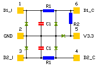
SWUSB-U3, SWUSBU3, SW USB-U3, SW USBU3, SW USB-3, SW USB3 USB UPSTREAM PORT FILTERS/ESD PROTECTION - PACUSB-U3, NUF2221W1T2 compatible. One upstream USB port terminator, EMI filter and transient overvoltage protector in a single surfacemount package Saves board space and lowers manufacturing costs compared to discret solutions ESD protection to 30 kV contact discharge per MIL-STD-883D, method 3015 ESD protection to 15 kV contact discharge per IEC6100-4-2 international standard ESD protection and termination of USB port All USB peripherals ( PC printers, scanners, zip drives, etc.) PDAs / handheld PCs Digital cameras Wireless Handets MP3 PlayerCable Modems The SWUSB-U3, SWUSBU3, SW USB-U3, SW USBU3, SW USB-3, SW USB3 are single-channel USB upstream-port termination networks.The SWUSB-U3, SWUSBU3, SW USB-U3, SW USBU3, SW USB-3, SW USB3 integrate EMI/RFI filter components R1 and C1, as recommended by the USB specification. Because these are upstream USB devices, they are terminated with a single 1.5 kW pull-up resistor to V3.3 (R2). There are three options for the value of the series resistor R1: for SWUSB-U1, R1 = 15ohms, for SWUSB-U2, R1 = 33ohms, for SWUSB-U3, R1 = 22ohms. This series resistance plus the USB driver output resistance must be close to the USB cable's characteristic impedance of 45W (90W balanced) to minimze transmission line reflections. In addition, these parts provide a very high level of protection for sensitive electronic components components that may be subjected to electrostatic discharge (ESD). The input and output pins are designed and characterized to dissipate ESD strikes of 15kV safely, a level well beyond the maximum requirements of the IEC 61000-4-2 international standard.Using the MIL-STD-883D (Method 3015) specification for Human Body Model (HBM) ESD, all pins are protected for contact discharges to greater than 30kV. PACUSB-U1, PACUSB-U2, PACUSB-U3, PAC USB-U1, PAC USB-U2, PAC USB-U3


SEMICONWELL
Integrated Passive Networks
  USB UPSTREAM PORT FILTERS/ESD PROTECTION
SWUSB-U3


FEATURES
APPLICATIONS
SCHEMATIC
One upstream USB port terminator, EMI filter and transient overvoltage protector in a single surfacemount package
Saves board space and lowers manufacturing costs compared to discret solutions
ESD protection to 30 kV contact discharge per MIL-STD-883D, method 3015
ESD protection to 15 kV contact discharge per IEC6100-4-2 international standard
ESD protection and termination of USB port
All USB peripherals ( PC printers, scanners, zip drives, etc.)
PDAs / handheld PCs
Digital cameras
Wireless Handets
MP3 Player
Cable Modems
schematic

SHORT PRODUCT APPLICATION NOTE
The SWUSB-U3 are single-channel USB upstream-port termination networks.
The SWUSB-U3 integrate EMI/RFI filter components R1 and C1, as recommended by the USB specification. Because these are upstream USB devices, they are terminated with a single 1.5 kW pull-up resistor to V3.3 (R2). There are three options for the value of the series resistor R1: for SWUSB-U1, R1 = 15W, for SWUSB-U2, R1 = 33W, for SWUSB-U3, R1 = 22W. This series resistance plus the USB driver output resistance must be close to the USB cable's characteristic impedance of 45W (90W balanced) to minimze transmission line reflections. In addition, these parts provide a very high level of protection for sensitive electronic components components that may be subjected to electrostatic discharge (ESD). The input and output pins are designed and characterized to dissipate ESD strikes of 15kV safely, a level well beyond the maximum requirements of the IEC 61000-4-2 international standard.
Using the MIL-STD-883D (Method 3015) specification for Human Body Model (HBM) ESD, all pins are protected for contact discharges to greater than 30kV.

SEMICONDUCTOR-THIN FILM MANUFACTURING PROCESS DESCRIPTION
Integrated passive networks are manufactured using advanced thin film technologies including ultra -stable and self passivating Tantalum Nitride resistors, gold interconnect metallization and reliable MNOS capacitors to achieve excellent uniformity, performance and reliability. Thin film resistor technology is the preferred solution for all applications that require low noise, long term stability and excellent performance at very high frequencies. Semiconwell employs proprietary thin film technologies for deposition of a wide range of sheet resistance films from 1W/sq to 10,000 W/sq. All Semiconwell's products are available in die form and as KGD, known good die and are ideal for high reliability hybrid and multi chip module applications. Besides thin film resistors, Semiconwell integrates capacitors, Schottky diodes, Zener diodes and transistors. Integrated passive and active networks are manufactured using Semiconwell's in house high reliability semiconductor manufacturing processes. All semiconductor devices employ precision doping via ion implantation, silicon nitride junction passivation, platinum silicided contacts and gold interconnect metallization for best performance and reliability. MNOS capacitors and Tantalum Nitride resistors are easily integrated with Schottky diodes to provide complete standard and custom RCD solutions. In die form, these products are ideal for hybrid and multi chip module applications. In packaged form, these products are the best solution where space and weight are a concern.

ABSOLUTE MAXIMUM RATINGS
Supply voltage Continuous IF Max DC Power to resistor Max Package Power
5.5V 100mA 100mW 200mW

Stresses beyond listed absolute maximum ratings may cause permanent damage to the device.

ELECTRICAL CHARACTERISTICS
PARAMETER VALUE UNITS
V3.3 (Supply voltage) <5.5 V
Operating Temperature Range -40 to 85 °C
Storage Temperature Range -65 to +150 °C
DC Power to Resistor 100 mW
Package Power 200 mW
Resistance R1±20% (SWUSB-U1 only) @ 25°C 22 W
Resistance R2±20% @ 25°C 1.5 KW
Capacitance C1±20%@ 1MHz, 2.5VDC, 25°C 47 pF
Diode Leakage (ILEAK) @ 3.3 VDC and 25°C <100 nA
Diode Reverse-biased Stand-off Voltage
(VD1) I=10mA, 25°C
min 5.5 V
Signal Clamp Voltage (VD2)
 Positive Clamp ±0.4V @10mA,
25°C
 Negative Clamp ±0.4V @ 10mA,
25°C

6.8

-0.8

V
V
In-system ESD Withstand Voltage (VESD)    
 Human Body Model, MIL-STD-883, Method3015  (Notes 1,2) ±30 kV
 IEC 61000-4-2, contact discharge method (I/O pins)  (Notes 1,2) ±15 kV
 IEC 61000-4-2, contact discharge method (V3.3 pin)  (Notes 1,2) ±25 kV
Clamping Voltage during ESD Discharge (VCLAMP) MIL-STD-883, Method 3015, 8kV; (Notes 1,2)
 Positive
 Negative

10
-5

V
V
Note 1: ESD applied to input/output V3.3 pins with respect to GND, one at a time. Clamping voltage is measured at the opposite side of the EMI filter to the ESD pin (i.e. if ESD is applied to pin 1, then clamping voltage is measured at pin 6). Unused pins are open.
Note 2: These parameters guaranteed by design.

PIN DESCRIPTION
LEAD NAME DESCRIPTION
1 D1i The USB controller side of the D+ or D- bidirectional transmission line of the differential pair defined by USB standards.
2 GND The ground reference for SWUSB-U3 device.
3 D2i The USB controller side of the D+ or D- bidirectional transmission line of the differential pair defined by USB standards.
4 D2c The connector side of the D+ or D- bidirectional transmission line of the differential pair defined by USB standards.
5 V3.3 The 3.3V supply voltage for the SWUSB-U3 device.
6 D1c The connector side of the D+ or D- bidirectional transmission line of the differential pair defined by USB standards.

GENERAL DIE INFORMATION
Substrate Thickness (mils) Die size (mils) Bonding pads Backside metal
SiO2 / Silicon 10±2 90 x 60 ±3 4x4 mils, 3mm thick, 99.99% electroplated gold with a TiW barrier Au/Si compatible with eutectic and conductive epoxy die attach.
All Semiconwell products are available in die form for chip and wire hybrid circuits and multi chip modules applications. Typical delivery for standard die products is 3-4 weeks ARO. For Chip Scale Packaged (CSP) devices consult factory for an update on availability of certain products.

DIODES RESISTORS CAPACITORS
Diodes offers basic ESD protection, with low forward voltage and low power dissipation. Diodes are small physically resulting low junction capacitance and low loading capacitance. Resistive material is ultra stable TaN with low TCR <75ppm/°C typical. For Rsq<10W/sq and Rsq>500W/sq, the resistive material is proprietary. Power rating/resistor max 100mW for R<1KW and 25mW for R>1KW. Standard tolerance is ±5%. Silicon nitride dielectric, MNOS capacitors exhibit high stability, low temperature coefficients, low leakage <10nA and high BV>50V.

DIE LAYOUT PACKAGE PIN OUT
layout image pending schematic
Vin=3,4,5,6,11,12,13,14
Vss=die backside
Vss=1,8,9,16
Vdd=2,7,10,15

STANDARD PRODUCTS ORDERING INFORMATION

R(W) SC70-6 SOT26 SOT326 BARE DIE
22 SWUSBU3-SC70 SWUSBU3-SOT26 SWUSBU3-SOT326 SWUSBU3-6BD

SW PART # QUANTITY SOT26 U/P($) SOT326 U/P($) BARE DIE U/P($)
SWUSB-U3   5,000pc -SOT26   -SOT326   -6BD  
SWUSB-U3 10,000pc -SOT26   -SOT326   -6BD  
For products sold as bare tested die or known good die KGD, minimum order is 5000pc. Dice are 100% functional tested, visual inspected and shipped in antistatic waffle packs. For special die level KGD requirements, different packaging or custom configurations, contact sw_sales@semiconwell.com

  Semiconwell P/N Quantity E-mail    
Receive Instant Quote
 

Delivery for packaged RCD standard products is 6-8 weeks ARO. Certain items may be available from stock. For standard products available from stock, there is a minimum line item order of $250.0. Inventory is periodically updated. For 2500pc or larger orders, all surface mount packaged devices are shipped in tape on reel (T/R). For smaller quantities, it may vary. Samples are available only for customers that have issued firm orders pending qualification of product in a particular application. On line Orders have to be verified, accepted and acknowledged by Semiconwell sales department in writing before, becoming non cancelable binding contracts.

Semiconwell guarantees continuous supply and availability of any of it's standard products provided minimum order quantities are met.

SEMICONWELL has made every effort to have this information as accurate as possible. However, no responsibility is assumed by SEMICONWELL for its use, nor for any infringements of rights of third parties which may result from its use. SEMICONWELL reserves the right to revise the content or modify its product line without prior notice. SEMICONWELL products are not authorized for and should not be used within support systems which are intended for surgical implants into the body, to support or sustain life, in aircraft, space equipment, submarine, or nuclear facility applications without the specific written consent.

Home Product Tree Tech. Support Print PDF Packages Request Quote Inventory Place Order Contact sales