|
PACUSB-D3 SWUSB-D3, SWUSBD1, SW USB-D3, SW USBD1, SW USB-1, SW USB1 USB DOWNSTREAM PORT TERMINATOR - from SEMICONWELL
USB DOWNSTREAM PORT TERMINATOR SWUSB-D3
FEATURES APPLICATIONS SCHEMATIC
A low-capacitance USB downstream port terminator,EMI filter, and transient over-voltage (ESD)protector in a single surface-mounted package ESD protection and termination of USB port
ESD protection to +20kV contact discharge, per MIL-STD-883D, Method 3015 All USB peripherals ( PC printers, scanners, zip drives, etc.)
ESD protection to +15kV contact discharge, per IEC 61000-4-2 International Standard PDAs / handheld PCs
Capacitors matched to a precision exceeding the USB specification Digital cameras
Compact SOT23-5 and SC70-5 package options save board space and lower manufacturing costs compared to discrete solutions Wireless Handets
MP3 Player Cable Modems
SHORT PRODUCT APPLICATION NOTE
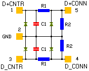
The SWUSB-D3 are single-channel USB downstream-port termination networks. The SWUSB-D3 integrate EMI/RFI filter components R1 and C1, as recommended by the USB specification as well as the required 15kW pull-down resistors (R2) to GND. In addition, PACUSB-D3/D2/D3 provides a very high level of protection for sensitive electronic components that may be subjected to electrostatic discharge (ESD). The device pins will safely dissipate ESD strikes of +15kV, exceeding the maximum requirements of the IEC 61000-4-2 international standard. Using the MILSTD-883D (Method 3015) specification for Human Body Model (HBM) ESD, all pins are protected from contact discharges to +20kV. There are three options for the value of the series resistor R1: 15W, 22W, and 33W. This series resistance, plus the USB driver output resistance, must be close to the USB cable’s characteristic impedance of 45 W(each side) to minimize transmission line reflections.
SEMICONDUCTOR-THIN FILM MANUFACTURING PROCESS DESCRIPTION
Integrated passive networks are manufactured using advanced thin film technologies including ultra -stable and self passivating Tantalum Nitride resistors, gold interconnect metallization and reliable MNOS capacitors to achieve excellent uniformity, performance and reliability. Thin film resistor technology is the preferred solution for all applications that require low noise, long term stability and excellent performance at very high frequencies. Semiconwell employs proprietary thin film technologies for deposition of a wide range of sheet resistance films from 1W/sq to 10,000 W/sq. All Semiconwell's products are available in die form and as KGD, known good die and are ideal for high reliability hybrid and multi chip module applications. Besides thin film resistors, Semiconwell integrates capacitors, Schottky diodes, Zener diodes and transistors. Integrated passive and active networks are manufactured using Semiconwell's in house high reliability semiconductor manufacturing processes. All semiconductor devices employ precision doping via ion implantation, silicon nitride junction passivation, platinum silicided contacts and gold interconnect metallization for best performance and reliability. MNOS capacitors and Tantalum Nitride resistors are easily integrated with Schottky diodes to provide complete standard and custom RCD solutions. In die form, these products are ideal for hybrid and multi chip module applications. In packaged form, these products are the best solution where space and weight are a concern.
ABSOLUTE MAXIMUM RATINGS
Supply voltage Continuous IF Max DC Power to resistor Max Package Power
6V 100mA 100mW 200mW
Stresses beyond listed absolute maximum ratings may cause permanent damage to the device.
ELECTRICAL CHARACTERISTICS
PARAMETER VALUE UNITS
V3.3 (Supply voltage) max 5.5 V
Operating Temperature Range -40 to 85 °C
Storage Temperature Range -65 to +150 °C
DC Power to Resistor 100 mW
Package Power 200 mW
Resistance R1 (SWUSB-D3 only) @ 25°C -20%(min.) 22(typ.) +20%(max.) W
Resistance R2 @ 25°C -20%(min.) 15(typ) +20%(max.) KW
Temperature Coefficient of Resistance +1300 ppm/°C
Capacitance C1@ 1MHz, 0VDC, 25°C -20%(min.) 47(typ.) +20%(max.) pF
Capacitance C1@ 1MHz, 2.5VDC, 25°C -20%(min.) 32(typ.) +20%(max.) pF
Diode Leakage (ILEAK) @ 3.3 VDC and 25°C 1(typ.) 100(max.) nA
Diode Reverse-biased Stand-off Voltage (VD1) I=10mA, 25°C min 5.5 V
Signal Clamp Voltage (VD2) Positive Clamp @10mA, 25°C Negative Clamp @ 10mA, 25°C 5.6 (min.) 6.8(typ.) 9.0(max.) -1.5 (min.) -0.8(typ.) -0.4(max.) V V
In-system ESD Withstand Voltage (VESD) Human Body Model, MIL-STD-883, Method3015 Pins 1, 3; Notes 2,3 and 4 Pins 4, 5; Notes 2 and 3 IEC 61000-4-2 Contact Discharge Pins 4, 5; Notes 2 and 3 ±4 ±20 ±15 kV
Clamping Voltage during ESD Discharge (VCLAMP) MIL-STD-883, Method 3015, 8kV; (Notes 2,5) Positive Negative 12 -7 V V
Note 1: Electrical operating characteristics guaranteed over standard operating conditions unless specified otherwise. Note 2: Guaranteed by design and characterization. Note 3: ESD voltage applied to pins with respect to GND, one at a time; unused pins are left open. Note 4: Pins 1 and 3 are not connected to the USB port connector, and therefore are not exposed to external ESD hazards. Thus,they do not require the high ESD protection levels provided for pins 4 and 5. Note 5: ESD Clamping Voltage is measured at the opposite end of R1 from the pin to which the ESD discharge is applied (e.g., if ESD is applied to pin 6, then the clamping voltage is measured at pin 1).
PIN DESCRIPTION
LEAD NAME DESCRIPTION
1 D+ CNTR D+ Data to the USB controller circuitry
2 GND Ground Pin
3 D- CNTR D- Data to the USB controller circuitry
4 D- CONN D- Data to the USB connector
5 D+ CONN D+ Data to the USB connector
|