|
SWPSSI3120CA same as NXP SEMICONDUCTORS PSSI3120CA PECL Positive Emitter-Coupled Logic CLOCK TERMINATION Silicon Si 20 x 40 mils manufactured by Semiconwell
SWPSSI3120CA same as NXP SEMICONDUCTORS PSSI3120CA PECL Positive Emitter-Coupled Logic CLOCK TERMINATION Silicon Si 20 x 40 mils manufactured by
Semiconwell SEMICONWELL PECL Positive Emitter-Coupled Logic CLOCK TERMINATION Integrated Passive Networks SWPSSI3120CA same as NXP SEMICONDUCTORS PSSI3120CA
FEATURES APPLICATIONS PECL Termination Single channel PECL termination in a three pin SOT23 package ESD protection
>2 kV Undershoot protection High capacitance range. Available in custom configurations and packages Enhances high
speed clock line signal integrity Workstations Desktop PCs Notebook PCs PECL Positive Emitter-Coupled Logic CLOCK
TERMINATION SWPSSI3120CA same as NXP SEMICONDUCTORS PSSI3120CA PRODUCT DESCRIPTION AND SHORT APPLICATION NOTE SWPSSI3120CA, Single channel, RC-type positive
emitter-coupled logic (PECL) clock termination with integrated diodes, providing electrostatic discharge (ESD)
protection up to 2 kV. Using thin film-on-silicon technology the PSSI3120CA integrates three resistors, one capacitor
and two diodes in a SOT23 package. The capacitor is protected from damage due to ESD by the diodes. The product is
designed to enhance signal integrity in clock distribution networks. Additionally, it can be used as a termination in
digital transmission lines where its inherent ESD protection helps maintain signal integrity by reducing undershoots.
TECHNOLOGY DESCRIPTION: SEMICONDUCTOR-THIN FILM MANUFACTURING All thin film microwave products are manufactured using
advanced semiconductors and thin film technologies including ultra-stable and self passivating Tantalum Nitride
resistors, gold interconnect metallization and reliable MNOS capacitors to achieve excellent uniformity, performance
and reliability. Thin film technology is the preferred solution for all applications that require low noise, long term
stability and excellent performance at very high frequencies. Semiconwell employs proprietary thin film technologies
for deposition of a wide range of resistive films with sheet resistance films from 1Ω/sq to 10,000Ω/sq. All Semiconwell
products are available in die form and are ideal for high reliability hybrid and multi chip module applications. All
Semiconwell products are manufactured using GOLD CHIP TECHNOLOGY™ a trade mark of Semiconix Corporation. ABSOLUTE
MAXIMUM RATINGS @ 25°C (unless otherwise stated) Parameter Symbol Value Unit Operating voltage V 5 V Continuous forward
current IF 10 mA Repetitive peak forward current IFRM 50 mA Storage temperature Tstg -60 to +150 °C Maximum junction
temperature Tj +150 °C Electrical Characteristics* TC = 25°C unless otherwise noted Name Symbol Test Conditions Value
Unit Min. Typ. Max R1, R2 resistance R1, R2 45 50 55 Ω R3 resistance R3 41.7 47 51 Ω C1 capacitance C1 120 180 pF
Thermal resistance from junction to ambient Rth-ja SOT23 standard mounting 500 K/W CROSS REFERENCE PARTS: GENERAL DIE
INFORMATION Substrate Thickness [mils] Size [mils] Bonding Pads Backside metal Silicon (Si) 10±0.5 40x20±2 min 4x4
mils, 3um thick, 99.99% electroplated gold with a TiW barrier Backside of the die is metallized with standard Ti/Pt/Au
compatible with Au-Sn, Au-Ge or silver filled conductive epoxy. Custom metallization is available for special orders.
All Semiconwell products are available in die form for chip and wire hybrid circuits and multi chip modules
applications. Typical delivery for standard die products is 3-4 weeks ARO. For Chip Scale Packaged (CSP) devices
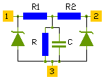
consult factory for an update on availability of certain products. PECL Termination DIE LAYOUT / MECHANICAL
SPECIFICATIONS PECL Positive Emitter-Coupled Logic CLOCK TERMINATION SWPSSI3120CA same as NXP SEMICONDUCTORS PSSI3120CA Pin # Function 1 IN/OUT 2 IN/OUT 3
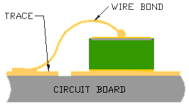
GND PECL Positive Emitter-Coupled Logic CLOCK TERMINATION SWPSSI3120CA PECL Termination CHIP MOUNT PECL Positive
Emitter-Coupled Logic CLOCK TERMINATION SWPSSI3120CA chip mount PECL Termination ASSEMBLY PROCESS - SHORT APPLICATION
NOTE Semiconwell standard bare die components are designed for thermosonic GOLD wire bonding and AuSi eutectic die
attach. For AuSn or AuGe die attach process, Ti/Pt/Au or Ti/Pd/Au are recommended backside metallization. For soft
solder die attach, backside metallization may be any of Ti/Ni/Au, Ti/Pt/Au, Ti/Pd/Au. For silver filled conductive
epoxy die attach, AuSi as well as Ti/Ni/Au, Ti/Pt/Au, Ti/Pd/Au may be used. In general, after die attach, prior to wire
bonding operation an oxygen RF plasma clean operation is recommended. IMPORTANT NOTE: Aluminum wire should not be used
with gold pads due to potential reliability problem known as purple plague. Same it applies to Aluminum bonding pads
with gold wire! In the transition from SnPb solder to lead free and RoHS compliant packaging and assembly processes the
reflow temperature has increased in some cases from 180°C to 220°C. This may cause an increase of the rate of formation
of gold aluminum intermetallic compounds that are brittle and are conducive to increased contact resistance and or bond
failure. STANDARD PRODUCTS ORDERING INFORMATION SW P/N PACKAGE MIN. QTY U/P [$] SWPSSI3120CA SOT23 Products sold for
space, military or medical applications, element evaluation and/or level K or S qualification are subject to minimum
order levels to be established on a case by case basis. For any special applications, die level KGD qualification
requirements, different packaging or custom configurations, contact sales department. INSTANT QUOTE Semiconwell P/N
Quantity E-mail ORDERING: Order on line at: http://www.semiconwell.com/purchase_order.htm. A copy of the order along
with an order confirmation receipt is issued instantly for all orders placed on line. On line Orders have to be
verified, accepted and acknowledged by Semiconwell sales department in writing before, becoming non cancelable binding
contracts. DELIVERY: Delivery for packaged Resistor networks standard products is 4-6 weeks ARO. Certain items may be
available from stock. For standard products available from stock, there is a minimum line item order of $250.0.
Inventory is periodically updated. For 2500pc or larger orders, all surface mount packaged devices are shipped in tape
on reel (T/R). For smaller quantities, it may vary. SHIPPING/PACKAGING: All devices for chip and wire applications are
100% tested, visual inspected and shipped in waffle packs (WP). For larger orders,>10k pc, devices can be shipped on
film frame. For smaller quantities, it may vary. For high volume automated assembly, devices may be supplied as 4"
wafers 100% tested, inked and diced on expanded film frame (FF). SAMPLES: Samples are available only for customers that
have issued firm orders pending qualification of product in a particular application. GUARANTEED SUPPLY! Semiconwell
guarantees continuous supply and availability of all standard products provided minimum order quantities are met.
Semiconwell has made every effort to have this information as accurate as possible. However, no responsibility is
assumed by Semiconwell for its use, nor for any infringements of rights of third parties which may result from its use.
Semiconwell reserves the right to revise the content or modify its product line without prior notice. Semiconwell
products are not authorized for and should not be used within support systems which are intended for surgical implants
into the body, to support or sustain life, in aircraft, space equipment, submarine, or nuclear facility applications
without the specific written consent of Semiconwell. Home Product Tree Tech. Support PDF
smxrootwww.semiconix.com/cgi-bin/rfq.cgi?site=&rows=1&item_1=SWPSSI3120CA&c_item_1=">Request Quote
Inventory
smxrootwww.semiconix.com/cgi-bin/order.cgi?site=&rows=1&item_1=SWPSSI3120CA&c_item_1=">Place Order
Contact sales Last updated: SEMICONWELL www.semiconwell.com Tel:(408)986-8026
Fax:(408)986-8027 ©1990- SEMICONWELL All rights reserved. No material from this site may be used or reproduced without
permission.
|