|
RT1401B RT1402B RT1403B RT1404B RT1405B RT1407B RT1408B same as SWDDR1A-CSP SDRAM-DDR Termination Array Chip Scale Package Ceramic manufactured by SEMICONWELL
CHIP SCALE FOR SDRAM - DDR TERMINATION ARRAY SWDDR1A-CSP
FEATURES
APPLICATIONS
18 Bit SSTL_2 Termination Sets
Ultra small footprint Chip Scale Package
Ceramic substrate
1.27mm Pitch
Compliant to JEDEC Std. 8-9
Ultra low channel capacitance
DDR Memory bus termination
SSTL Termination
SHORT PRODUCT APPLICATION NOTE
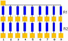
The SWDDR-CSP is a high performance integrated Passive Device which provides Series/Parallel terminations suitable for use in SSTL and DDR termination applications. Nine Series/Parallel termination channels are provided for a total of 18 integrated resistors. These resistors provide excellent high frequency performance in excess of 3 GHz and are manufactured to an absolute tolerance of ±1%. The Chip Scale Package provides an ultra small footprint for this Integrated Passive Devices and provides minimal parasitics compared toconventional packaging. Typical bumps inductance is less than 25pH. The large solder bumps and ceramic substrate allow for standard attachment to laminate printed circuit boards without the use of underfill. The 3x9 Bump pattern is arranged for easy flow through routing on the pcb.
SEMICONDUCTOR-THIN FILM MANUFACTURING PROCESS DESCRIPTION
Integrated passive networks are manufactured using advanced thin film technologies including ultra -stable and self passivating Tantalum Nitride resistors, gold interconnect metallization and reliable MNOS capacitors to achieve excellent uniformity, performance and reliability. Thin film resistor technology is the preferred solution for all applications that require low noise, long term stability and excellent performance at very high frequencies. Semiconwell employs proprietary thin film technologies for deposition of a wide range of sheet resistance films from 1 W/sq to 10,000 W/sq. All Semiconwell's products are available in die form and as KGD, known good die and are ideal for high reliability hybrid and multi chip module applications. Besides thin film resistors, Semiconwell integrates capacitors, Schottky diodes, Zener diodes and transistors. Integrated passive and active networks are manufactured using Semiconwell's in house high reliability semiconductor manufacturing processes. All semiconductor devices employ precision doping via ion implantation, silicon nitride junction passivation, platinum silicided contacts and gold interconnect metallization for best performance and reliability. MNOS capacitors and Tantalum Nitride resistors are easily integrated with Schottky diodes to provide complete standard and custom RCD solutions. In die form, these products are ideal for hybrid and multi chip module applications. In packaged form, these products are the best solution where space and weight are a concern.
RESISTOR SPECIFICATIONS
Capacitance [pF] Tolerance q [%] Power Rating [mW]
<0.20pF 1, 5, 10 50 mW@70°C
Stresses beyond listed absolute maximum ratings may cause permanent damage to the device.
ELECTRICAL CHARACTERISTICS
PARAMETER VALUE UNITS
Resistor Value R1=60 ; R2=25 W
Resistor Value R1=50 ; R2=25 W
Resistor Value R1=25 ; R2=22 W
Resistor Tolerance ±1.0 %
MaximumResistor Power,at 70°C 0.05 W
Temperature Coefficient of Resistance ±100 ppm/°C
Operating Temperature Range -40°C to +85 °C
GENERAL DIE INFORMATION
Substrate Thickness (mils) Die size (mils) Bonding pads Backside metal
Al2O3 99.6 % 15±2 450x150±3 4x4 mils, 3mm thick, 99.99% electroplated gold with a TiW barrier Au/Si compatible with eutectic and conductive epoxy die attach.
All Semiconwell products are available in die form for chip and wire hybrid circuits and multi chip modules applications. Typical delivery for standard die products is 3-4 weeks ARO. For Chip Scale Packaged (CSP) devices consult factory for an update on availability of certain products.
CONDUCTORS RESISTORS BACKSIDE METAL
0.35mm Dia. Bumps Resistive material is ultra stable TaN with low TCR <75ppm/°C typical. For Rsq<10W/sq and Rsq>500W/sq, the resistive material is proprietary. Power rating/resistor max 100mW for R<1KW and 25mW for R>1KW. Standard tolerance is ±5%. Backside of the die is metallized with standard Si/Au compatible with eutectic and epoxy die attach. Custom metallizations are available upon special request for die products only.
DIE LAYOUT PACKAGE PIN OUT
Vin=3,4,5,6,11,12,13,14
Vss=die backside
Vss=1,8,9,16
Vdd=2,7,10,15
STANDARD PRODUCTS ORDERING INFORMATION
R1(W) R2(W) CSP BARE DIE
60 25 SWDDR1A/600/250-CSP SWDDR1A/600/250-BD
50 25 SWDDR1A/500/250-CSP SWDDR1A/500/250-BD
25 22 SWDDR1A/250/220-CSP SWDDR1A/250/220-BD
SW PART # QUANTITY CSP U/P($) BARE DIE U/P($)
SWDDR1A/600/250-1% 5,000pc -CSP -BD
SWDDR1A/600/250-1% 5,000pc -CSP -BD
List prices are for standard products, available from stock. List prices for other quantities and tolerances are available on line through Instant Quote. For standard products available from stock, there is a minimum line item order. For custom products please inquire by contacting SEMICONWELL technical sales. No rights can be derived from pricing information provided on this website. Such information is indicative only, is showed for budgetary use only and subject to change by SEMICONWELL at any time and without notice.
For custom products sold as bare tested die or known good die KGD, minimum order is 5000pc. Dice are 100% functional tested, visual inspected and shipped in antistatic waffle packs. For special die level KGD requirements, different packaging or custom configurations, contact sw_sales@semiconwell.com
INSTANT QUOTE Semiconwell P/N Quantity E-mail
SWDDR1A-CSP/600/250 SWDDR1A-CSP/500/250 SWDDR1A-CSP/250/220 -5% -1% -CSP -BD
Delivery for packaged Resistor networks standard products is 4-6 weeks ARO. Certain items may be available from stock. For standard products available from stock, there is a minimum line item order of $250.0. Inventory is periodically updated. For 2500pc or larger orders, all surface mount packaged devices are shipped in tape on reel (T/R). For smaller quantities, it may vary. Samples are available only for customers that have issued firm orders pending qualification of product in a particular application. On line Orders have to be verified, accepted and acknowledged by Semiconwell sales department in writing before, becoming non cancelable binding contracts.
Semiconwell guarantees continuous supply and availability of any of it's standard products provided minimum order quantities are met.
SEMICONWELL has made every effort to have this information as accurate as possible. However, no responsibility is assumed by SEMICONWELL for its use, nor for any infringements of rights of third parties which may result from its use. SEMICONWELL reserves the right to revise the content or modify its product line without prior notice. SEMICONWELL products are not authorized for and should not be used within support systems which are intended for surgical implants into the body, to support or sustain life, in aircraft, space equipment, submarine, or nuclear facility applications without the specific written consent.
|
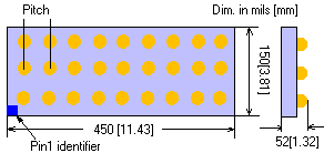 1.27mm [50 mils] pitch