CM1210-02 same as SWDL002 2 CHANNELS VERY LOW CAPACITANCE ESD PROTECTION DIODE NETWORK manufactured by SEMICONWELL SWDL002 2 CHANNELS Very LOW CAPACITANCE ESD PROTECTION DIODE NETWORK FEATURES 2 channels of ESD protection, Very low loading capacitance, 1pF typical, +6 kV ESD protection per channel (IEC 61000-4-2 standard), Available in SOT23 and SC70 package APPLICATIONS USB 2.0 ports at 480Mbps, IEEE1394 Firewire ports at 400 Mbps, Gigabit Ethernet ports, Flat panel display interfaces, Wireless antennas, General purpose high-speed data line ESD protection 
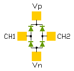
SHORT PRODUCT APPLICATION NOTE The SWDL002 family of diode array have been designed to provide ESD protection for electronic components or sub-systems requiring minimal capacitive loading. These devices are ideal for protecting systems with high data and clock rates or for circuits requiring low capacitive loading. Each ESD channel consists of a pair of diodes which will steer the ESD current pulse to either the positive (VP) or negative (VN) supply rail. The SWDL will protect against ESD pulses up to +6kV per the IEC61000-4-2 standard.This device is particularly well-suited for systems using high-speed port implementations such as USB2.0, IEEE1394, (Firewire,i.Link), Gigabit Ethernet and corresponding ports in removable storage, digital camcorders, DVD-RW drives and other applications where extremely low loading capacitance with ESD protection are required in a small package footprint. SEMICONDUCTOR-THIN FILM MANUFACTURING PROCESS DESCRIPTION Integrated passive networks are manufactured using advanced thin film technologies including ultra -stable and self passivating Tantalum Nitride resistors, gold interconnect metallization and reliable MNOS capacitors to achieve excellent uniformity, performance and reliability. Thin film resistor technology is the preferred solution for all applications that require low noise, long term stability and excellent performance at very high frequencies. Semiconwell employs proprietary thin film technologies for deposition of a wide range of sheet resistance films from 1W/sq to 10,000 W/sq. All Semiconwell's products are available in die form and as KGD, known good die and are ideal for high reliability hybrid and multi chip module applications. Besides thin film resistors, Semiconwell integrates capacitors, Schottky diodes, Zener diodes and transistors. Integrated passive and active networks are manufactured using Semiconwell's in house high reliability semiconductor manufacturing processes. All semiconductor devices employ precision doping via ion implantation, silicon nitride junction passivation, platinum silicided contacts and gold interconnect metallization for best performance and reliability. MNOS capacitors and Tantalum Nitride resistors are easily integrated with Schottky diodes to provide complete standard and custom RCD solutions. In die form, these products are ideal for hybrid and multi chip module applications. In packaged form, these products are the best solution where space and weight are a concern. ABSOLUTE MAXIMUM RATINGS Maximum supply voltage 6V Continuous, IF 8mA/diode, Max Power dissipation 225mW@70°C/package STANDARD SPECIFICATIONS (All parameters specified at T A =25°C unless otherwise noted.) Operating Temperature Range -40 to +85 °C Storage Temperature Range -65 to +150 °C DC Voltage at any channel input (VN - 0.5) to (VP + 0.5) V Operating Supply Voltage (VP - VN) 0 to 5.5 V Channel Leakage Current typ ±0.1 max ±1 µA Diode Forward Voltage, VF @IF=8mA min 0.60 typ. 0.8 max 0.95 V Channel Input Capacitance @ 1 MHz, VP=3.3V Vin=1.65V;(Note 1) typ.1 max. 1.3 pF ESD PROTECTION Peak discharege Voltage at any channel input, in system; contact discharge per IEC61000-4-2 standard (Note1,2,4, TA=25°C) min. ±6 kV Channel clamp voltage at 8kV ESD HBM (Note 1,2,3) Positive Transients Negative Transients max. VP+10.0 max. VN-10.0 V Note1: These parameters guaranteed by design and characterization. Note2: From I/O pins to VP or VN only. VP bypassed to VN with a 0.22µF ceramic capacitor. Note3: Human Body Model per MIL-STD-883, Method 3015, Cdisharge=100pF, Rdischarge=1.5kW, VP=3.3V, VN=grounded. Note4: Standard IEC61000-4-2 with Cdischarge=150pF, Rdischarge=330W, VP=3.3V, VN=grounded


SEMICONWELL
Integrated Passive Networks
  2 CHANNELS VERY LOW CAPACITANCE ESD PROTECTION DIODE NETWORK
SWDL002


FEATURES
APPLICATIONS
SCHEMATIC
2 channels of ESD protection
Very low loading capacitance, 1pF typical
+6 kV ESD protection per channel (IEC 61000-4-2 standard)
Available in SOT143 and SC70 package
 
 
USB 2.0 ports at 480Mbps
IEEE1394 Firewire ports at 400 Mbps
Gigabit Ethernet ports
Flat panel display interfaces
Wireless antennas
General purpose high-speed data line ESD protection
schematic

SHORT PRODUCT APPLICATION NOTE
The SWDL family of diode array have been designed to provide ESD protection for electronic components or sub-systems requiring minimal capacitive loading. These devices are ideal for protecting systems with high data and clock rates or for circuits requiring low capacitive loading. Each ESD channel consists of a pair of diodes which will steer the ESD current pulse to either the positive (VP) or negative (VN) supply rail. The SWDL will protect against ESD pulses up to +6kV per the IEC61000-4-2 standard.This device is particularly well-suited for systems using high-speed port implementations such as USB2.0, IEEE1394, (Firewire,i.Link), Gigabit Ethernet and corresponding ports in removable storage, digital camcorders, DVD-RW drives and other applications where extremely low loading capacitance with ESD protection are required in a small package footprint.

SEMICONDUCTOR-THIN FILM MANUFACTURING PROCESS DESCRIPTION
Integrated passive networks are manufactured using advanced thin film technologies including ultra -stable and self passivating Tantalum Nitride resistors, gold interconnect metallization and reliable MNOS capacitors to achieve excellent uniformity, performance and reliability. Thin film resistor technology is the preferred solution for all applications that require low noise, long term stability and excellent performance at very high frequencies. Semiconwell employs proprietary thin film technologies for deposition of a wide range of sheet resistance films from 1W/sq to 10,000 W/sq. All Semiconwell's products are available in die form and as KGD, known good die and are ideal for high reliability hybrid and multi chip module applications. Besides thin film resistors, Semiconwell integrates capacitors, Schottky diodes, Zener diodes and transistors. Integrated passive and active networks are manufactured using Semiconwell's in house high reliability semiconductor manufacturing processes. All semiconductor devices employ precision doping via ion implantation, silicon nitride junction passivation, platinum silicided contacts and gold interconnect metallization for best performance and reliability. MNOS capacitors and Tantalum Nitride resistors are easily integrated with Schottky diodes to provide complete standard and custom RCD solutions. In die form, these products are ideal for hybrid and multi chip module applications. In packaged form, these products are the best solution where space and weight are a concern.

ABSOLUTE MAXIMUM RATINGS
Maximum supply voltage VP-VN Continuous IF Max Power dissipation
6V 8mA/diode 225mW@70°C/package

Stresses beyond listed absolute maximum ratings may cause permanent damage to the device.

STANDARD SPECIFICATIONS (All parameters specified at T A =25°C unless otherwise noted.)
PARAMETER VALUE UNITS
Operating Temperature Range -40 to +85 °C
Storage Temperature Range -65 to +150 °C
DC Voltage at any channel input (VN - 0.5) to (VP + 0.5) V
Operating Supply Voltage (VP - VN) 0 to 5.5 V
Channel Leakage Current typ ±0.1 max ±1 µA
Diode Forward Voltage, VF @IF=8mA min 0.60 typ. 0.8 max 0.95 V
Channel Input Capacitance @ 1 MHz, VP=3.3V Vin=1.65V;(Note 1) typ.1 max. 1.3 pF
ESD PROTECTION
Peak discharege Voltage at any channel input, in system; contact discharge per IEC61000-4-2 standard (Note1,2,4, TA=25°C) min. ±6 kV
Channel clamp voltage at 8kV ESD HBM (Note 1,2,3)
Positive Transients
Negative Transients

max. VP+10.0
max. VN-10.0
V
Note1: These parameters guaranteed by design and characterization.
Note2: From I/O pins to VP or VN only. VP bypassed to VN with a 0.22µF ceramic capacitor.
Note3: Human Body Model per MIL-STD-883, Method 3015, Cdisharge=100pF, Rdischarge=1.5kW, VP=3.3V, VN=grounded.
Note4: Standard IEC61000-4-2 with Cdischarge=150pF, Rdischarge=330W, VP=3.3V, VN=grounded

GENERAL DIE INFORMATION
Substrate Thickness (mils) Die size (mils) Bonding pads Backside metal
SiO2 / Silicon 10±2 90 x 60 ±3 4x4 mils, 3mm thick, 99.99% electroplated gold with a TiW barrier Au/Si compatible with eutectic and conductive epoxy die attach.
All Semiconwell products are available in die form for chip and wire hybrid circuits and multi chip modules applications. Typical delivery for standard die products is 4-6 weeks ARO. For Chip Scale Packaged (CSP) devices consult factory for an update on availability of certain products.

DIODES BONDING PADS CAPACITORS
Junction diodes are solid state devices designed specifically for transient suppression. Low capacitance compensation diode in series with TVS diode provides a low capacitance solution. The bonding pads are 3µm thick, 99.99% electroplated gold with a TiW barrier that withstands 30 min at 400°C in air without loss of adhesion. Silicon nitride dielectric, MNOS capacitors exhibit high stability, low temperature coefficients, low leakage <10nA and high BV>50V.

DIE / PACKAGE LAYOUT PACKAGE PIN OUT
layout / design pending schematic
SOT143: 1-Vn, 2-Vp, 3-CH2, 4-CH1
SC70-4: 4-Vn, 1-Vp, 2-Ch2, 3-Ch1
Vss=1,8,9,16
Vdd=2,7,10,15

STANDARD PRODUCTS ORDERING INFORMATION

PART # SOT143 SC70-4
SWDL002 SWDL002-SOT143 SWDL002-4SC

SW PART # QUANTITY SOT143 U/P($) SC70-4 U/P($)
SWDL002   5,000pc -SOT143   -4SC  
SWDL002 10,000pc -SOT143   -4SC  
For products sold as bare tested die or known good die KGD, minimum order is 5000pc. Dice are 100% functional tested, visual inspected and shipped in antistatic waffle packs. For special die level KGD requirements, different packaging or custom configurations, contact sw_sales@semiconwell.com

  Semiconwell P/N Quantity E-mail    
Receive Instant Quote
 

Delivery for packaged RCD standard products is 6-8 weeks ARO. Certain items may be available from stock. For standard products available from stock, there is a minimum line item order of $250.0. Inventory is periodically updated. For 2500pc or larger orders, all surface mount packaged devices are shipped in tape on reel (T/R). For smaller quantities, it may vary. Samples are available only for customers that have issued firm orders pending qualification of product in a particular application. On line Orders have to be verified, accepted and acknowledged by Semiconwell sales department in writing before, becoming non cancelable binding contracts.

Semiconwell guarantees continuous supply and availability of any of it's standard products provided minimum order quantities are met.

SEMICONWELL has made every effort to have this information as accurate as possible. However, no responsibility is assumed by SEMICONWELL for its use, nor for any infringements of rights of third parties which may result from its use. SEMICONWELL reserves the right to revise the content or modify its product line without prior notice. SEMICONWELL products are not authorized for and should not be used within support systems which are intended for surgical implants into the body, to support or sustain life, in aircraft, space equipment, submarine, or nuclear facility applications without the specific written consent.

Home Product Tree Tech. Support Print PDF Packages Request Quote Inventory Place Order Contact sales