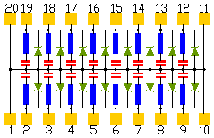
RCD16-47B6, RCD16-47B6RL , 16 RCD LINE TERMINATION is pin to pin compatible with SWRCD/470/330-20SOW and SWRCD/470/330-20QS. ESD Protected RCD Network for Bus Termination Network of 16 RCD line terminations Resistance : R=47ohms, tolerance ±10%, Capacitance: C=33 pF, tolerance ±10% Schottky diode (D) Provides impedance matching, thus increasing noise immunity and minimizing distortion. Lowers EMI / RFI radiation. Uses the best of all termination schemes. No DC power dissipation. Eliminates negative voltages: no current will change the bias of the protected device. In any electronic equipment where a suitable bus terminationis requiredto avoid signal reflectionsand distortions: PC and workstation computer. Data-line analyzers. With the increasing speed of data transmission, line reflections provide signal distorsions and the overshootsor undershootsproduced on the signal edges can cause the malfunction of the whole system .To avoid these negative effects from leading to problems, a suitable termination is required. Dedicated to bus termination, theSWRCD16provides by far the best method to minimise stray emissions from PCB tracks. SEMICONWELL Advanced Integrated Passive Networks Diode protected RC termination network SWRCD FEATURES APPLICATIONS 1,6,12,13,19,24 - VSS High frequency performance 9 termination lines/package AC Termination Low pass filter PRODUCT DESCRIPTION These products are integrated thin film resistor-networks that are designed to suppress transmission line effects on high speed data lines. The series solution improves performance and reduces assembly cost on passive components. The RCD series allows the loads to be attached anywhere along the line, with no DC power dissipation. These products are manufactured using advanced thin film technologies including ultra-stable and self passivating Tantalum Nitride resistors, gold interconnect metalization and reliable MNOS capacitors to achieve excellent uniformity, performance and reliability. In die form, these products are ideal for hybrid and multichip module applications. In packaged form, these products are the best solution where space and weight are a concern. SEMICONDUCTOR-THIN FILM MANUFACTURING PROCESS DESCRIPTION Integrated passive networks are manufactured using advanced thin film technologies including ultra-stable and self passivating Tantalum Nitride resistors, gold interconnect metallization and reliable MNOS capacitors to achieve excellent uniformity, performance and reliability. Thin film resistor technology is the preferred solution for all applications that require low noise, long term stability and excellent performance at very high frequencies. Semiconwell employs proprietary thin film technologies for deposition of a wide range of sheet resistance films from 1W/sq to 10,000 W/sq. All Semiconwell's products are available in die form and are ideal for high reliability hybrid and multi chip module applications. SUBSTRATE INFORMATION RESISTOR SPECIFICATIONS Material Thickness (mil) Min. die size (mils) Power rating Tolerance q % Capacitance SiO2 / Silicon 10±2 90 x 60 ±3 50 mW@70°C 1, 5, 10 <5pF RESISTORS CONDUCTORS BACKSIDE METALS Resistive material is ultra stable TaN with low TCR <75ppm/°C typical. For Rsq<10W/sq and Rsq>500W/sq, the resistive material is proprietary. Power rating/resistor max 100mW for R<1Kohm and 25mW for R>1Kohm. Standard tolerance is ±5%. The bonding pads are 3µm thick, 99.99% electroplated gold with a TiW barrier that withstands 30 min at 400°C in air without loss of adhesion. Backside of the die is metallized with standard Si/Au compatible with eutectic and epoxy die attach. Custom metallizations are available upon special request for die products only. SCHEMATIC DIE LAYOUT 1,6,12,13,19,24 - VSS


SEMICONWELL
Integrated Passive Networks
  ESD PROTECTED RCD NETWORK FOR BUS TERMINATION
SWRCD


FEATURES
APPLICATIONS
SCHEMATIC
Network of 16 RCD line terminations
Resistance : R=47W, tolerance ±10%, Capacitance: C=33 pF, tolerance ±10%
Schottky diode (D) Provides impedance matching, thus increasing noise immunity and minimizing distortion.
Lowers EMI / RFI radiation.
Uses the best of all termination schemes. No DC power dissipation.
Eliminates negative voltages : no current will change the bias of the protected device.
In any electronic equipment where a suitable bus terminationis requiredto avoid signal reflectionsand distortions:
PC and workstation computer.
Data-line analyzers.


schematic

SHORT PRODUCT APPLICATION NOTE
SWRCD series, provide adequate termination in applications where signal reflections and distortions are not acceptable like data analyzers, computers and workstations.

SEMICONDUCTOR-THIN FILM MANUFACTURING PROCESS DESCRIPTION
Integrated passive networks are manufactured using advanced thin film technologies including ultra -stable and self passivating Tantalum Nitride resistors, gold interconnect metallization and reliable MNOS capacitors to achieve excellent uniformity, performance and reliability. Thin film resistor technology is the preferred solution for all applications that require low noise, long term stability and excellent performance at very high frequencies. Semiconwell employs proprietary thin film technologies for deposition of a wide range of sheet resistance films from 1 W/sq to 10,000 W/sq. All Semiconwell's products are available in die form and as KGD, known good die and are ideal for high reliability hybrid and multi chip module applications. Besides thin film resistors, Semiconwell integrates capacitors, Schottky diodes, Zener diodes and transistors. Integrated passive and active networks are manufactured using Semiconwell's in house high reliability semiconductor manufacturing processes. All semiconductor devices employ precision doping via ion implantation, silicon nitride junction passivation, platinum silicided contacts and gold interconnect metallization for best performance and reliability. MNOS capacitors and Tantalum Nitride resistors are easily integrated with Schottky diodes to provide complete standard and custom RCD solutions. In die form, these products are ideal for hybrid and multi chip module applications. In packaged form, these products are the best solution where space and weight are a concern.

ABSOLUTE MAXIMUM RATINGS
Reverse voltage VR Continuous IF IFRM for tw<100ms Max Power dissipation
7.5V 50mA 100 mA (20%duty cycle) 100mW@70°C/channel

Stresses beyond listed absolute maximum ratings may cause permanent damage to the device.

ELECTRICAL CHARACTERISTICS
PARAMETER VALUE UNITS
Total power dissipation per package 500 mW
Continuous forward current per Schottky diode 50 mA
Repetitive peak reverse voltage 7.5 V
Maximum electrostatic discharge MIL STD 883C-Method 3015-6 2 kV
Storage temperature range -55 to +150 °C
Maximum junction temperature 150 °C
Connection resistance (note1),Tamb=25°C max 0.25 W
Total capacitance @ f=1MHz, VR=0V, VRMS=30mV typ. 45 pF
Leakage current @ VR=VRRM, Tj=25°C max 1 µA
Leakage current @ VR=VRRM, Tj=70°C max 10 µA
Forward voltage @ IF=1mA, Tj=25°C max 0.5 V
Forward voltage @ IF=16mA, Tj=25°C max 1.0 V
 
Note 1 : Rc is the resistance between pin 1 and pin 11 or between pin 10 and pin 20.

GENERAL DIE INFORMATION
Substrate Thickness (mils) Die size (mils) Bonding pads Backside metal
SiO2 / Silicon 10±2 72 x 58 ±3 4x4 mils, 3mm thick, 99.99% electroplated gold with a TiW barrier Au/Si compatible with eutectic and conductive epoxy die attach.
All Semiconwell products are available in die form for chip and wire hybrid circuits and multi chip modules applications. Typical delivery for standard die products is 3-4 weeks ARO. For Chip Scale Packaged (CSP) devices consult factory for an update on availability of certain products.

DIODES RESISTORS CAPACITORS
Schottky diodes offer basic ESD protection, with low forward voltage, low leakage and low power dissipation in OFF state. Schottky Diodes exhibit low junction capacitance CTand low on resistance RDON. Resistive material is ultra stable TaN with low TCR <75ppm/°C typical. For Rsq<10W/sq and Rsq>500W/sq, the resistive material is proprietary. Power rating/resistor max 100mW for R<1KW and 25mW for R>1KW. Standard tolerance is ±5%. Silicon nitride dielectric, MNOS capacitors exhibit high stability, low temperature coefficients, low leakage <10nA and high BV>50V.

DIE/PACKAGE LAYOUT SCHEMATIC DIAGRAM
VARIES AS A FUNCTION OF PACKAGE
layout
schematic
I/O=2-9,12-19
Vss=die backside
Vss=1,10,11,20
Vdd=2,7,10,15

STANDARD PRODUCTS ORDERING INFORMATION

R(W) C(pF) RC  CODE SW PART# SOICW-20 QSOP-20 BARE DIE-20
47 33 470/330 SWRCD/470/330 -SOW20 -QS20 -BD20

SW PART # QUANTITY SOICW-20 U/P($) QSOP-20 U/P($) BARE DIE U/P($)
SWRCD/470/330   5,000pc -20SOW $2.15 -20QS $2.15 -20BD $2.65
SWRCD/470/330 10,000pc -20SOW $1.93 -20QS $1.93 -20BD $2.43
For products sold as bare tested die or known good die KGD, minimum order is 5000pc. Dice are 100% functional tested, visual inspected and shipped in antistatic waffle packs. For special die level KGD requirements, different packaging or custom configurations, contact sw_sales@semiconwell.com

INSTANT QUOTE
Semiconwell P/N Quantity E-mail    
 

Delivery for packaged RCD standard products is 6-8 weeks ARO. Certain items may be available from stock. For standard products available from stock, there is a minimum line item order of $250.0. Inventory is periodically updated. For 2500pc or larger orders, all surface mount packaged devices are shipped in tape on reel (T/R). For smaller quantities, it may vary. Samples are available only for customers that have issued firm orders pending qualification of product in a particular application. On line Orders have to be verified, accepted and acknowledged by Semiconwell sales department in writing before, becoming non cancelable binding contracts.

Semiconwell guarantees continuous supply and availability of any of it's standard products provided minimum order quantities are met.

SEMICONWELL has made every effort to have this information as accurate as possible. However, no responsibility is assumed by SEMICONWELL for its use, nor for any infringements of rights of third parties which may result from its use. SEMICONWELL reserves the right to revise the content or modify its product line without prior notice. SEMICONWELL products are not authorized for and should not be used within support systems which are intended for surgical implants into the body, to support or sustain life, in aircraft, space equipment, submarine, or nuclear facility applications without the specific written consent.

Home Product Tree Tech. Support Print PDF Packages Request Quote Inventory Place Order Contact sales