|
SWDL1230-08CSP same as CM1230-08CS, LOW CAPACITANCE ESD PROTECTION ARRAY SWDL1230-08-CSP
FEATURES 2 channels of ESD protection Provides ESD protection to IEC61000-4-2 Level 4 ±8kV contact discharge;±15kV air discharge, Low loading capacitance of 0.8pF typical, Minimal capacitance change with temperature and voltage, Channel I/O to GND capacitance difference of 0.02pF typical is ideal for differential signals,Channel I/O to I/O capacitance 0.15pF typical
APPLICATIONS LCD and Camera data lines in wireless handsets that use high-speed serial interfaces, I/O port protection for mobile handsets, notebook computers, DSCs, MP3 players, PDAs, etc. including USB, 1394 and Serial ATA, Wireless handsets,LCD and camera modules,Handheld PCs/PDAs
SHORT PRODUCT APPLICATION NOTE
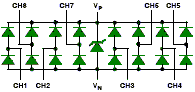
SWDL1230 series are ideal for protecting systems with high data and clock rates or for circuits that require low capacitive loading. Each channel consists of a pair of ESD diodes that act as clamp diodes that steer positive or negative ESD current pulses to either the positive or negative supply rail. A zener diode is integrated into the array between the positive and negative supply rails. The VCC rail is thus protected from ESD strikes and eliminates the need for a bypass capacitor to absorb positive ESD strikes to ground. Each channel of the SWDL1230 can safely dissipate ESD strikes of ±8kV, meeting the Level 4 requirement of the IEC61000-4-2 international standard for contact discharges as well as ±15kV air discharges per the IEC61000-4-2 specification. Using the MIL-STD-883 (Method 3015) specification for Human Body Model (HBM) ESD, the pins are protected for contact discharges at greater than ±15kV.This device is particularly well-suited for next generation wireless handsets that implement high-speed serial interface solutions for the LCD display and camera interfaces. In these wireless handset designs, a tolerance above 1.5pF cannot be tolerated due to the high data rates that are transferred between the baseband chipset and the LCD driver/controller ICs because a higher capacitive loading will cause the rise and fall times to slow which in turn hampers the functionality of circuit and operation of the wireless handset.
SEMICONDUCTOR-THIN FILM MANUFACTURING PROCESS DESCRIPTION
Integrated passive networks are manufactured using advanced thin film technologies including ultra -stable and self passivating Tantalum Nitride resistors, gold interconnect metallization and reliable MNOS capacitors to achieve excellent uniformity, performance and reliability. Thin film resistor technology is the preferred solution for all applications that require low noise, long term stability and excellent performance at very high frequencies. Semiconwell employs proprietary thin film technologies for deposition of a wide range of sheet resistance films from 1 W/sq to 10,000 W/sq. All Semiconwell's products are available in die form and as KGD, known good die and are ideal for high reliability hybrid and multi chip module applications. Besides thin film resistors, Semiconwell integrates capacitors, Schottky diodes, Zener diodes and transistors. Integrated passive and active networks are manufactured using Semiconwell's in house high reliability semiconductor manufacturing processes. All semiconductor devices employ precision doping via ion implantation, silicon nitride junction passivation, platinum silicided contacts and gold interconnect metallization for best performance and reliability. MNOS capacitors and Tantalum Nitride resistors are easily integrated with Schottky diodes to provide complete standard and custom RCD solutions. In die form, these products are ideal for hybrid and multi chip module applications. In packaged form, these products are the best solution where space and weight are a concern.
ABSOLUTE MAXIMUM RATINGS
Operating Supply Voltage (VP - VN) 6V, Operating Temperature Range -40 to +85°C, Storage Temperature Range -65 to +150°C,DC Voltage at any channel input (VN - 0.5) to (VP + 0.5) V
ELECTRICAL CHARACTERISTICS
PARAMETER VALUE UNITS
Operating Supply Voltage (VP-VN) typ.3.3 max.5.5 V
Operating Supply Current,(VP-VN)=3.3V max.8 µA
Diode Forward Voltage,IF = 8mA; TA=25°C min.0.6 typ.0.8 max.0.95 V
Channel Leakage Current,TA=25°C; VP=5V, VN=0V,VIN = 0V to 5V typ.± 0.1 max.± 1.0 µA
Channel Input Capacitance,1 MHz, VP=3.3V, VN=0V,VIN=1.65V; Note 2 typ.0.8 max. 1.20 pF
Channel Input Capacitance Matching,1 MHz, VP=3.3V, VN=0V,VIN=1.65V; Note 2 typ. 0.02 pF
Mutual Capacitance between signal pin and adjacent signal pin typ.0.15 pF
In-system ESD Protection Peak Discharge Voltage at any channel input, in system a) Contact discharge per IEC 61000-4-2 standard,Notes 2, 4 & 5 b) Human Body Model, MILSTD-883, Method 3015,Notes 2, 3 & 5 min.±8 min±15 V V
Channel Clamp Voltage Positive Transients Negative Transients typ.+9.8 typ.-1.8 V V
Dynamic Resistance,IPP = 1A, tP = 8/20µS,Any I/O pin to Ground; Note 2 and 5 Positive Transients Negative Transients typ.0.76 typ.0.56 V V
Note 1: T A =25°C unless otherwise specified Note 2:These parameters guaranteed by design and characterization. Note 3: Human Body Model per MIL-STD-883, Method 3015, CDischarge = 100pF, RDischarge = 1.5KO, VP = 3.3V, VN grounded. Note 4: Standard IEC 61000-4-2 with CDischarge = 150pF, RDischarge = 330O, VP = 3.3V, VN grounded. Note 5: These measurements performed with no external capacitor on VP. Note 6: Measured under pulsed conditions, pulse width = 0.7ms, maximum current = 1.5A.
|